Research
Laboratory Overview
Thin-film materials, characterized by their “thinness,” are widely used in our daily lives, including electronic devices. We are conducting research and development aiming at making materials more functional and energy-efficient by utilizing nanostructures and nanolayers. For example, we are focusing on silver thin film, which has the best features of low resistivity and high reflectivity among all metallic materials, and are developing highly stable silver thin film that can maintain the original electrical and optical properties of silver by introducing a nanometer-scale surface layer to suppress aggregation under heating and high humidity environments. Extremely thin silver thin films also play an important role in ecoglasses, which are effective for energy conservation in buildings. On the other hand, nanostructures and nanolayers exhibit optical properties and functionality unique to the nanoscale, unlike objects of normal size. We are also conducting research on improving the performance of organic light-emitting diodes using multilayer nanolayers and on increasing the efficiency of light-emitting devices using the plasmon emission amplification phenomenon of patterning metallic nano-materials.
Research Themes of the Laboratory
Professor Midori Kawamura
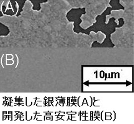
Preparation of highly stable silver thin films by layering surface nanolayers
Silver thin films have promising applications as low-E coatings and reflective mirrors in various optical devices due to their low emissivity and high reflectivity. However, there are stability issues, for example, agglomeration phenomenon occurs upon heating, resulting in degradation of physical properties. To overcome this problem, we have developed silver thin films with excellent heat-resistant aggregation properties by introducing surface and interface nanolayers. We are also clarifying which materials are suitable as nanolayers and why.
Fabrication of high performance thin films utilizing interfacial nanolayers
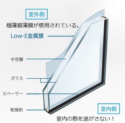
Ecoglass (double glazing low-E glass) coated with a functional thin film to reduce heat inflow and loss through window glass is attracting attention. This makes cooling in summer and heating in winter more efficient. Ultra-thin silver thin films play an important role here, but various innovations are needed to produce thin films with high quality. Our goal is to achieve higher energy savings through the accumulation of films utilizing nanolayers.
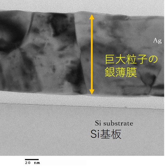
Crystal growth by krypton sputtering
In the sputtering method, which is widely used in industry, thin metal films are deposited in argon plasma. Argon ions knock out atoms on the metal surface and deposit metal atoms on the substrate. At the same time, however, we have observed a phenomenon in which a small amount of argon is also incorporated into the film. We have found that, for example, when silver films are deposited in krypton plasma, crystal growth is enhanced and films with excellent electrical properties are obtained.
Associate Professor Takayuki Kiba
Development of Functional Multilayer Thin Films for High Performance OLED Devices
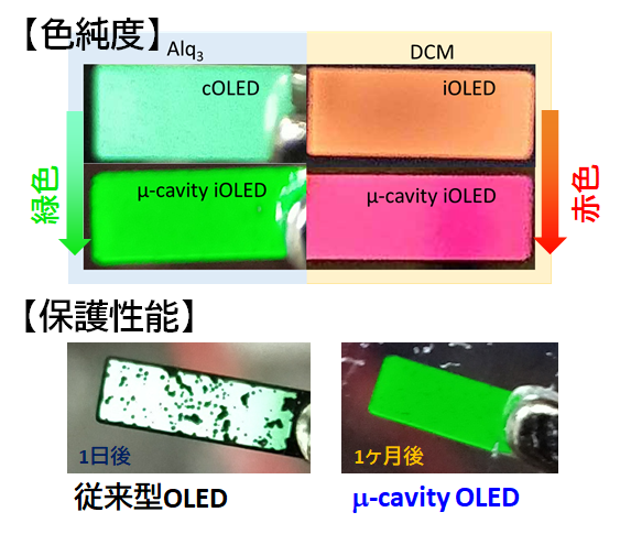
Organic light-emitting diodes (OLEDs) are once again attracting attention and demand is increasing for display applications in smartphones, televisions, and other devices. While their application is advancing, organic light-emitting materials generally suffer from low color purity and rapid degradation due to their susceptibility to water and moisture. We have proposed a new structure that combines the sharpness of the emission spectrum and encapsulation performance against water vapor and oxygen, and are aiming to achieve higher performance.
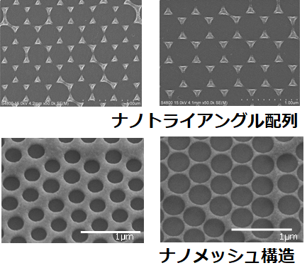
Fabrication of metallic nanostructures using a simple lithographic technique and their luminescence amplification effect
Free electrons on metal surfaces and in nanostructures oscillate cooperatively differently from those in the bulk, resulting in unique optical properties and functionality never seen before. In particular, nanostructures fabricated by metal microfabrication can be expected to exhibit efficient light extraction and photoelectric field enhancement effects for various wavelengths of light. We have fabricated metal nanostructures using nanosphere lithography with polystyrene bead arrays as templates and verified the light emission enhancement phenomenon.
Metal-Semiconductor Hybrid Nanostructures for Highly Efficient Light-Emitting Devices
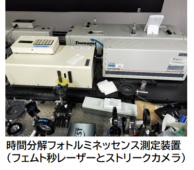
We are incorporating the aforementioned metallic nanostructures into light-emitting devices to improve the luminescence efficiency due to their localized surface plasmons. We are designing nanostructures to match the emission wavelength and optimizing the structure to maintain and exhibit the luminescence amplification effect without interfering with current injection. We are also investigating the mechanism of luminescence amplification in devices by real-time measurement (=time-resolved laser spectroscopy) of luminescence phenomena that occur within a short period of time (pico-(10^-12)-nano-(10^-9)-seconds).