Research
Overview
Thin-film materials are widely used in everyday electronic devices because of their “thin” form factor and versatile functions. Our laboratory conducts research and development to enhance material functionality and energy efficiency by utilizing nanostructures and nanoscale layers (nanolayers).
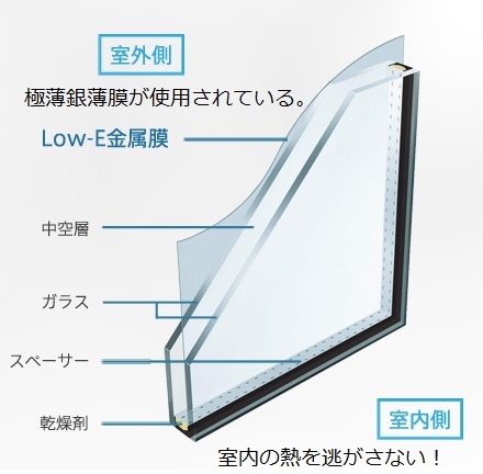
For example, we focus on silver (Ag) thin films, which exhibit the lowest electrical resistivity and high reflectivity among metals. By introducing nanoscale surface and interfacial layers, we suppress Ag aggregation under heating or high-humidity conditions and develop highly stable Ag thin films that preserve Ag’s intrinsic electrical and optical properties. Ultra-thin Ag films also play a key role in energy-saving architectural glazing (Low-E insulated glass).
In nanostructures and nanolayers, unique optical and functional properties emerge at the nanoscale, which differ from those of bulk materials. We also study high-performance organic EL devices using multilayer nanolayers and high-efficiency light-emitting devices based on plasmon-enhanced emission from patterned metallic nanostructures.
Research Topics
Prof. Midori Kawamura
Highly stable Ag thin films enabled by surface/interfacial nanolayers
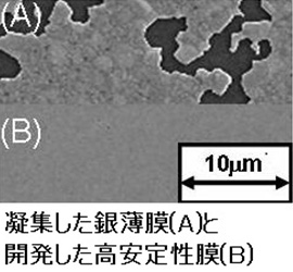
Ag thin films are attractive as electrodes and reflective mirrors due to high conductivity and high reflectivity; however, single-layer Ag films often suffer from limited stability (e.g., thermal dewetting/aggregation). We developed Ag thin films with excellent resistance to such degradation by introducing surface and interfacial nanolayers, and we investigate suitable nanolayer materials and underlying mechanisms.
High-performance energy-saving thin films via nanolayer stacking
Low-emissivity (Low-E) insulated glass coated with functional thin films has attracted attention for reducing heat gain/loss through windows, improving cooling efficiency in summer and heating efficiency in winter. Ultra-thin Ag films are essential in these coatings, but high-quality fabrication requires careful engineering. We aim to realize higher energy-saving performance by stacking optimized nanolayers.
Crystal growth control by selecting noble gases for sputtering processes
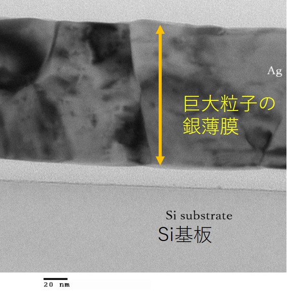
In sputtering, metal atoms are ejected and deposited using noble-gas plasmas (typically Ar). It is also known that a small amount of noble gas may be incorporated into the film. We study how appropriate noble-gas selection promotes film crystallization depending on the metal; for example, Ag films deposited in Kr plasma can show enhanced crystal growth and improved electrical properties, and we clarify the presence/absence of noble-gas incorporation.
Prof. Takayuki Kiba
Functional multilayer thin films for high-performance organic EL devices
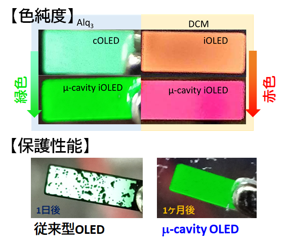
Organic EL devices are widely used in smartphones and TVs, and their demand continues to grow. However, organic emitters often face issues such as limited color purity and vulnerability to water/moisture. We propose metal–dielectric hybrid multilayer structures deposited on devices to sharpen emission spectra and improve encapsulation performance against moisture and oxygen, aiming to enhance device performance.
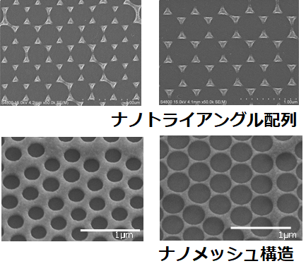
Metal nanostructure fabrication and emission enhancement using simple lithography
Collective electron oscillations on metal surfaces and in nanostructures can exhibit unique optical properties not found in bulk materials. Patterned metallic nanostructures are expected to enable efficient light extraction and strong local field enhancement across various wavelengths. We fabricate metallic nanostructures using nanosphere lithography with self-assembled polystyrene beads as templates and investigate emission enhancement phenomena.
High-efficiency light-emitting devices based on metal–semiconductor hybrid nanostructures
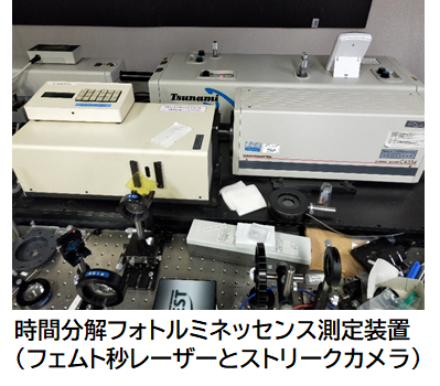
By integrating the above metallic nanostructures into light-emitting devices, we aim to improve emission efficiency via localized surface plasmon effects. We optimize nanostructure designs matched to emission wavelengths and develop structures that maintain enhancement effects without hindering current injection. We also use time-resolved laser spectroscopy (picosecond–nanosecond timescales) to elucidate emission-enhancement mechanisms in devices.